An active antenna design for civil GPS (fcenter = 1,575 GHz) is done using the possibilities of 3d LDS fabrication to integrate antenna and Low Noise Amplifier (LNA) directly on one plastic part. To further improve the functionality a slotted patch antenna combined with a 3d modulation of the substrate surface is used. The proposed antenna is targeted to provide an input matching better than 10 dB in a 50 Ω system. A right handed circular polarization (RHCP) with an axial ratio (AR) of less than 3 dB in the upper half space should be obtained.
First of all, the slotted patch antenna is evaluated and optimized for the targeted application on a planar substrate. In the next step the patch antenna is applied on different modulated surfaces and matched again. The modulation described is done folding the whole antenna substrate including the ground plane side showing the possibilities of the 3D MID fabrication. The resulting space under the modulated antenna can be used to integrate a circuit layout as it is done for the LNA in the following design.
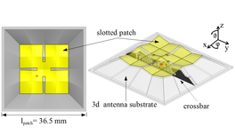
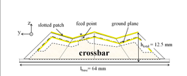
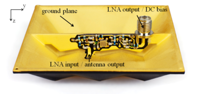
The antenna surface is modulated under the patch surface as it can be seen in the side view (Fig. 1(c)). Besides the surface modulation directly underneath the patch surface the side parts are folded down and a bit outwards (Fig. 1(c)) to obtain some extra space to integrate the LNA circuit later on. Optimizing the antenna leads to a total height of htotal = 12.5 mm and a length of the base area of lbase = 64 mm. The length of the modulated patch is lpatch = 36.5 mm and the height due to patch modulation is hpatch = 3 mm. The resulting
space under the antenna is used to install a small crossbar on which the circuit elements can be placed on. This crossbar is fixed only at three points not to interrupt the metallization of the ground plane underneath the patch face with the main surface current distribution. The antenna`s functionality is only slightly influenced by this procedure. One fixed point in the middle of the crossbar is used to root the feeding point of the antenna to the input of the following LNA circuit as depicted in Fig. 1(c).
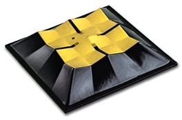
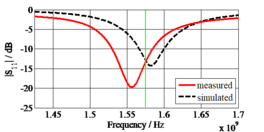
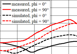
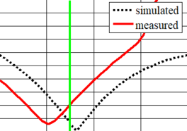
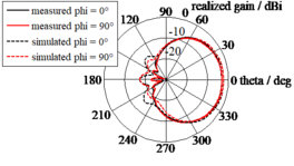
A prototype antenna is realized is shown in Fig. 2. The fabrication is done using LPKF ProtoPaint LDS on a stereolithographic part. The antenna is measured and simulated onto an aluminium plate of 250 × 250 × 3 mm. Fig. 3(a) shows the simulated and measured return loss of the antenna. In the targeted frequency range an input matching better than 10 dB is obtained, marked with a line. The resonance frequency measured and simulated differs about 25 MHz. This may be caused by differences in the resulting permittivity of the LDS varnished epoxy resin. The evaluation of the radiation characteristics is done at the respective resonance frequency. The radiation characteristics in Fig. 3(b) show a good agreement between the measured and simulated results. The maximum antenna gain is about -2.5 dBi at the zenith. Fig. 3(c) shows that the AR is minimal at resonance frequency for both, the measured and the simulated values. An AR of 1.5 dB is obtained in simulations and 2.8 dB for the measured structure.
The 3D antenna design allows the integration of circuit components like an LNA or matching network close to the feeding point. For an active antenna the integration of the LNA close to the feeding point is of particular importance for the reduction of the system noise figure. Another aspect illustrating the advantages of the 3D antenna design described here is that the ground plane of the patch antenna additionally shields the circuit on the crossbar against electromagnetic interferences. The low signal strengths in GPS applications show the importance of this fact.
For the design of the LNA a two-stage approach is used. For the layout of the LNA circuit the integration space has to be considered. This means in detail that the circuit design has to fit on the crossbar and has to be realizable with LDS ProtoPaint. The backside of the crossbar is metalized and connected to the patch antenna ground. Thus, the patch antenna and the LNA circuit have the same ground reference.
The gain in the desired frequency range is about 36 dB (simulated) and 28.3 dB (measured). Referred to the carrier the attenuation at the cell phone communication frequencies is about 73 dB at 827.5 MHz and 55 dB at 1885 MHz. The 1dB compression point is about P1dB,IN = 19.9 dBm. The measured In-Band IIP3 is IIP3 = - 5,1 dBm for the input signals f1 = 1.574 GHz und f2 = 1.576 GHz with an input power of Pin = -35 dBm. A comparison of these results with those of an automotive compliant commercial LNA for GPS shows that the designed LNA provides comparable characteristics. In addition the circuit design is fully integrated under the 3D patch antenna and realizable with the 3D LDS method. All in all the discussed active antenna is a good example, showing the possibilities of the 3D MID technology to enhance antenna and circuit design for the future demands on radio systems, especially for automotive applications.
References
[1] A. Friedrich, L. Berkelmann, T. Martinelli, B. Geck, O. Klemp, I. Kriebitzsch (2015): An Active Three-Dimensional GPS Patch Antenna Using MID-Technology, European Microwave Conference 2015 (EuMC 2015), Paris, France, September 7 - 11, 2015
[2] O. Klemp, A. Friedrich, B. Geck, A. Posselt (2014): 3D-Antennensysteme - Anforderungen an die Fahrzeugintegration, ATZ - Automobiltechnische Zeitschrift 116, Springer Vieweg, Nr. 12, S. 60-65


