Over the past funding period within the framework of the Collaborative Research Centre 653 (CRC 653), researchers from Institute of Microwave and Wireless Systems pursued different concept and technologies for the implementation of an electric device equipped with the feature to establish a wireless bidirectional communication.
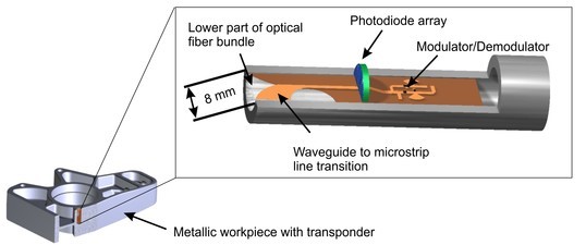
In the first funding period (2005 - 2009) the principal feasibility of the RFID technology was established, and a passive unidirectional communication was realized [1]. The integrated circuit was power supplied by the microwave field of the reader. In the second funding period (2009 - 2013) a wireless bidirectional communication with a transmission range of 0.5 m was achieved. A reduction of the transponder dimensions down to Ø 8 mm x 26 mm was strived [2, 3]. For this reason, the transmission frequency had to be increased to 24 GHz. Since the power supply could not be provided by the electromagnetic field of the read/write unit, an optoelectronic converter (photodiode array) and a light source have been added. It was proven that the combination of microwave data transmission and optical supply yields an outstanding performance gain compared to the first funding period, thus the range of functions has increased significantly (see Figure 1).


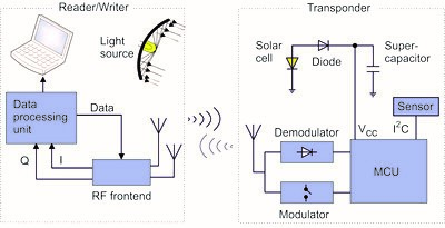
In order to develop a wide range of applications, new concepts and technologies shall be attempted in the current funding period (2013 - 2017) [4]. A block diagram of the developed wireless communication system is depicted in Fig. 2. The reading/writing unit is shown on the left-hand side while the communication module, also called as transponder, is illustrated on the right-hand side.


To realize our vision, a highly integrated multi-layer composition of electrical and optical components shall be implemented. The design concept of an optoelectronic integrated RF communication module for the integration into metallic components is illustrated in Figure 3. Hereby, new challenges are occurring in terms of mounting and connection technology as well as the development of an optically transparent high frequency circuit including an antenna.
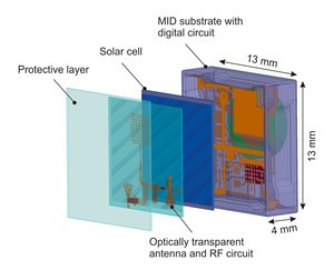


The exploded view shows the highly integrated multi-layer structure. This module consists of four main parts. A housing is needed to carry the individual layers. A promising approach is the use of three dimensional molded interconnect devices (3D-MID) acting as circuit carriers. By means of the laser direct structuring (LDS) process electronic conducting paths can be created directly on the plastic compounds.
The proposed housing has a volume of 13 x 13 x 4 mm³. On the backside of this housing, space is available for the integration of a digital circuit consisting of an ultra-low power microcontroller and an energy storage. Additional sensors such as an acceleration sensor is integrated within the module to expand its scope of functions. To connect the digital circuit with other layers through hole vias are used. This production step can be realized completely within the LDS process. Hereby, the laser drills through the plastic compounds and at the subsequent metallization process copper deposits in the hole. In this way, a reliable connection can be achieved.
To power the digital unit an energy harvesting concept consisting of a high efficient multijunction solar cell with an efficiency of 40 % is used. Thus, an external light source such as a halogen lamp or sufficient ambient light is necessary in order to supply electrical power to the communication module. Thanks to the supercapacitor acting as an energy storage and the use of low-power components the communication module is able to process and transmit data for several minutes in a complete darkness condition.
The wireless communication is based on the backscatter modulation principle and operates in the 24 GHz industrial scientific and medical (ISM) radio band. The RF circuit including a patch antenna is arranged above the solar cell. Therefore, the suitability of optically transparent and conductive materials was studied. The reciprocal influences of the solar cell and the RF structure were analysed which led to further challenges in the design of the patch antenna as well as the RF circuit.
In order to communicate and to exchange data with the communication module, a reading/writing unit is needed. This unit consists of a FPGA-based data processing unit from National Instrument and commercially available RF modules, which are evaluated in details and connected to each other. The two main parts are the digital unit and the analog unit. The digital unit generates data for the transmitting path and interprets the incoming signals from the communication module. All of these tasks can be controlled via a graphical user interface, which is developed within this subproject. The programming of the data processing unit as well as the graphical user interface (GUI) is realized by the development environment LabVIEW. The performance such as the communication distance of the whole communication system is evaluated in our laboratory. The transmitted power of the reading/writing unit is set to 20 dBm ERP (100 mW effective radiated power, radio regulation). The antenna of the reading/writing unit is aligned with the communication module. Considering the laboratory environment the maximum communication distance is determined up to 2 meters depending on the gain of the receiving antenna.
Referenzen
[1] E. B. Kaldjob, Design and Analysis of Field-powered Transponders Integrated in Metallic Objects, Dissertation Leibniz Universität Hannover, 2010.
[2] J. Meyer, Ein optisch versorgter RFID-Transponder für die Integration in Metall, Dissertation Leibniz Universität Hannover, Berichte aus dem HFT. Garbsen: PZH - Produktionstechnisches Zentrum GmbH, 2015.
[3] J. Meyer, Q.H. Dao, B. Geck (2014): 24 GHz RFID Communication System for Product Lifecycle Applications, in: Proc. 2nd International Conference on System-Integrated Intelligence: Challenges for Product and Production Engineering, SysInt 2014, July 2nd -4th, Bremen, Germany, 2014, pp. 369-375.
[4] Q. H. Dao, B. Geck (2020): Optically Transparent 24 GHz Analog Front-End Based on Meshed Microstrip Lines for the Integration in a Self-Sufficient RFID Sensor Tag, in IEEE Journal of Radio Frequency Indetification, vol. 4, Issue 2, pp. 83-92, June 2020, DOI: 10.1109/JRFID.2019.2954471


