The efficiency enhancement of the Doherty amplifier is also based on the effect, that the voltage swing is maximized at all output power levels, but the load modulation is done automatically through an interaction of two transistors.
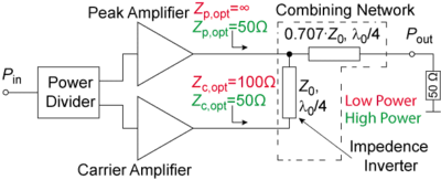
The classical Doherty architecture consists of two single amplifiers, the so called carrier and peak amplifier. The power divider splits the input signal into both of them. At the output both amplifiers are connected over a combing network to a common load of \(Z_L=50 Ω\) , whereas the combing network consists of an impedance inverter and a matching network.
The impedance inverter is usually implemented as a microstrip-line with the characteristic impedance of optimal load impedance of the carrier and the peak amplifier \(Z_{opt}=Z_{c,opt}=Z_{p,opt}\) and a phase shift of uneven multiples of 90°. The performance of the Doherty amplifier can be divided into two parts, the low power (LP) and the high power (HP) range.
In the low power range only the carrier amplifier is active, due to the defined bias points of both amplifiers and an higher RF input power for the carrier amplifier, the latter being realized by the power divider. Hence, the input signal of the peak amplifier is smaller than its threshold voltage. In this range the carrier amplifier is terminated with \(Z_{c,opt}=100 Ω\) and the peak amplifier provides \(Z_{p,opt}=∞\) due to the combining network for the center frequency \(f_0\).
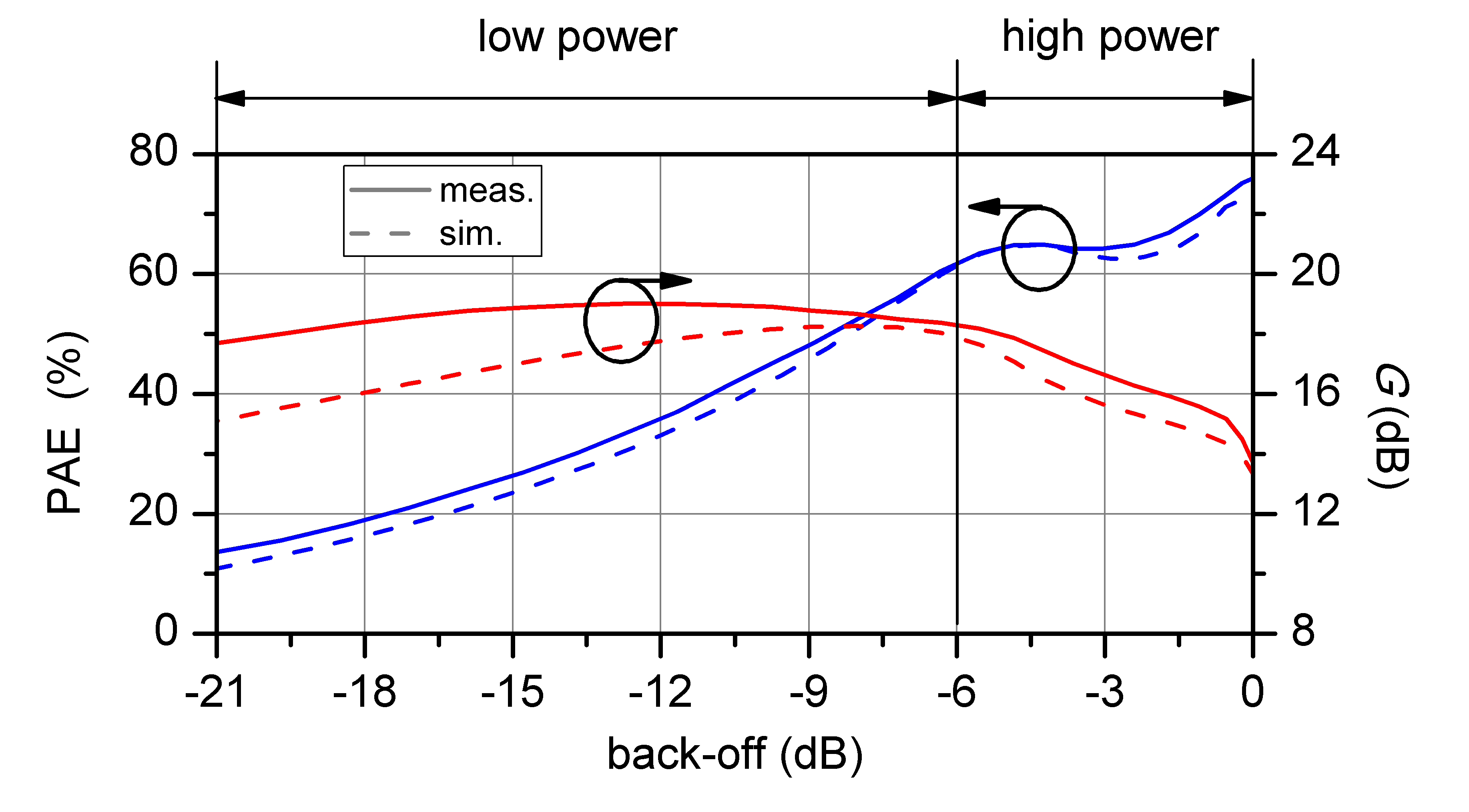
In the high power range the efficiency only varies by a small amount depending of the back-off, whereas a slight efficiency drop exists dependent on the load modulation of the carrier amplifier and the power ratio of the carrier and the peak amplifier.
The optimal load of the carrier amplifier \(2Z_{c,opt}=100 Ω \) (LP) decreases for increasing output power \(Z_{c,opt}\) (HP), because the peak amplifier begins to amplify. In this case, for maximal output power, both amplifiers have the same optimal load impedance \(Z_{c,opt}=Z_{p,opt}=50 Ω\). This load modulation of the carrier amplifier enhances the overall efficiency of the Doherty amplifier.
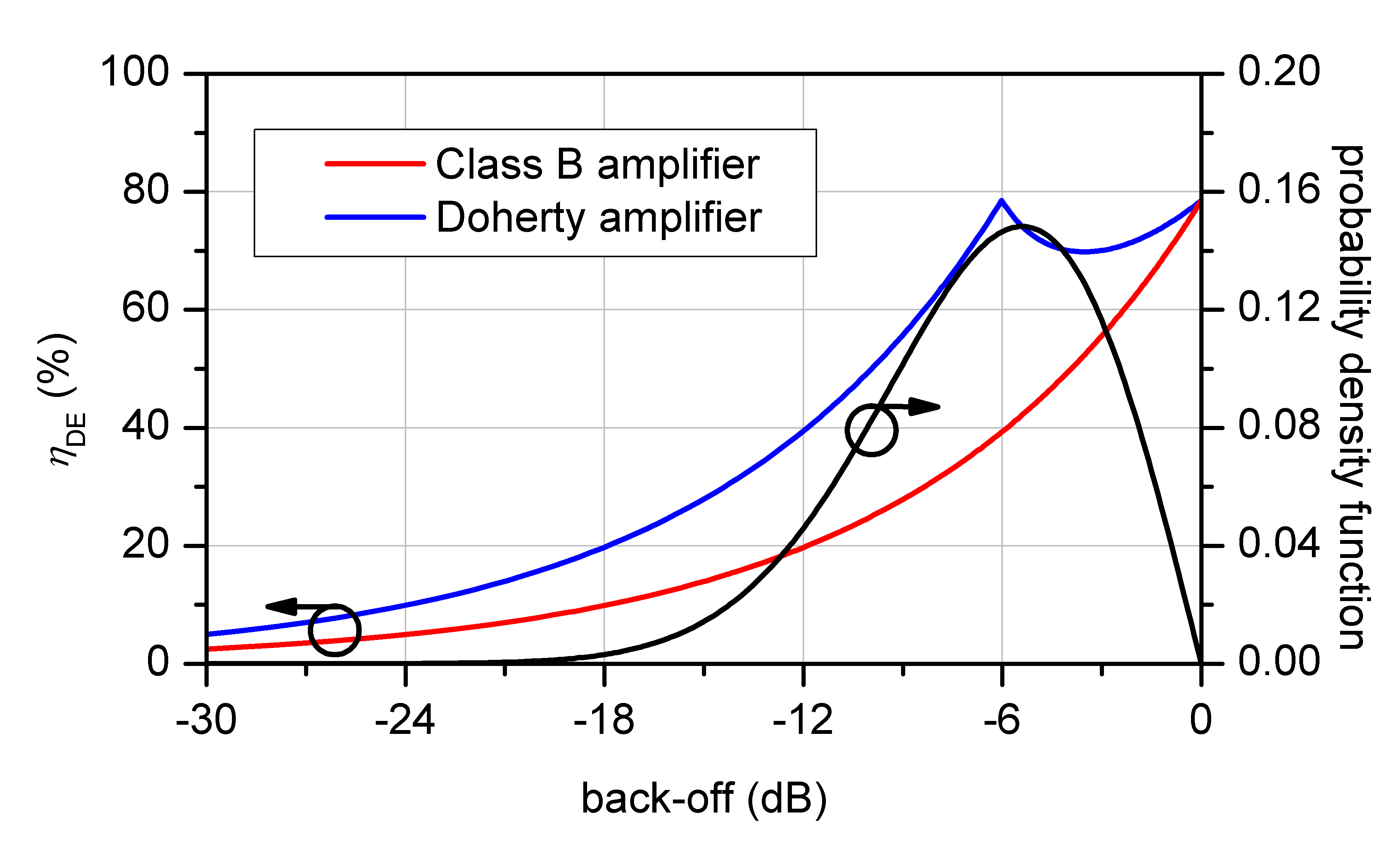
Fig. 8 shows comparison of a signal transistor solution, in this case a Class B power amplifier and a Doherty power amplifier. Furthermore, the probability density function of a 64 QAM signal is shown in this figure. The highest probability of the amplitude is below the maximal signal power, but the class B amplifier has the highest efficiency at the highest output power.
The PAE and the gain of a realized 1 GHz Doherty amplifier is presented in Fig. 9. The used Doherty amplifier is based on inverse Class F amplifier for a high over absolute efficiency.
Reference
[1] S. Probst, E. Denicke, B. Geck (2017): In Situ Waveform Measurement within a Doherty Power Amplifier Under Operational Conditions, IEEE Transactions on Microwave Theory and techniques, Vol. 65, No. 6, pp. 2192 - 2200, June 2017
DOI: 10.1109/TMTT.2017.2651809


