


Transmitter and Receiver Circuits
Modern communication systems, e.g. a mobile transmitter or a base station, place strict requirements on linearity and efficiency. The radio frequency power amplifier of a base station is the part with the highest DC power consumption. In stationary as well as in mobile communication system applications the DC power consumption of the RF power amplifier affects the cooling complexity, the battery lifetime and with it the costs of the setup. Therefore, the maximal efficiency of the power amplifiers should be increased, e.g. through the use of Class F or inverse Class F. The increase in efficiency is achieved only at the maximum RF output power. An efficiency enhancement over the dynamic range is furthermore necessary through the high peak-to-average power ratio (PAPR) of the complex modulation scheme. A possible approach to enhance the efficiency for signals is the Doherty power amplifier. The efficiency requirement comply with the Doherty power amplifier. The linearity of the efficient power amplifier can be improved through a digital predistortion (DPD).
The Institute of Microwave and Wireless Systems is working within the topics of efficient power amplifiers and waveform engineering respectively nonlinear measurement techniques.
Efficient Power Amplifiers
In general a power amplifier has the highest efficiency at maximum output power near the saturation region. However, through the high peak-to-average power ratio, which result in modern communication systems with high data rates, a high efficiency in the back-off range is required. The efficiency can be enhanced with different techniques and topologies.
A possible solution to enhance the efficiency in the range of the average power is a variation of the load impedance of the transistor. This variation can be realized with an adaptive matching network or automatically with a Doherty amplifier.
-
Dual-Input-Doherty
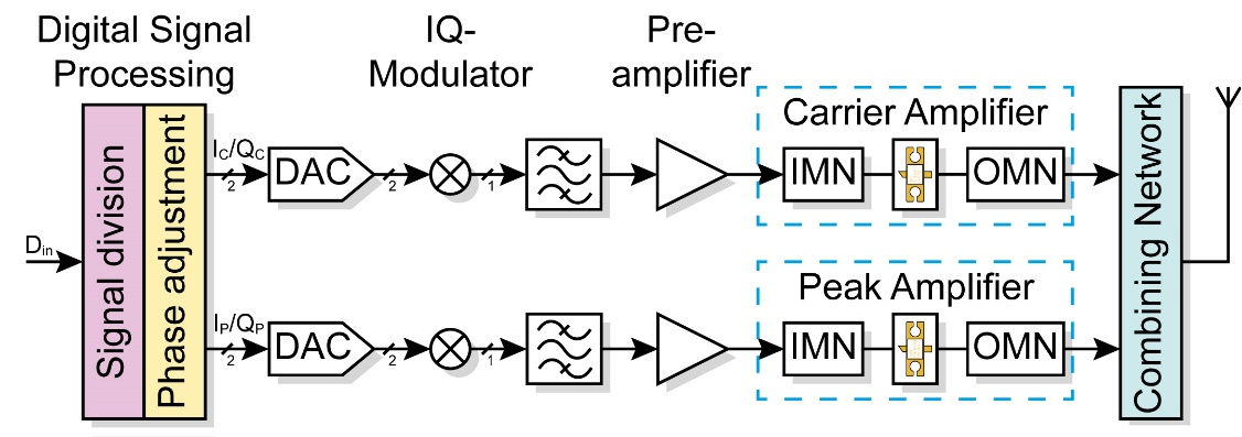
In order to enhance the efficiency of the Doherty amplifier over its full range, the discrete input divider with fixed signal distribution can be removed and each amplifier can be supplied with a signal, that carries the same information but is adjusted in amplitude and phase depending on the input power. The schematic structure of this dual-input Doherty amplifier architecture is shown in Fig. 10.
![]()
![]()
![]()
Fig. 10: Block diagram of the Dual-Input-Doherty amplifier architecture For this type of signal distribution, two preamplifier sections are required, what makes it possible to double the maximum input power. The signal division is shifted to the digital domain. Every input sample can be modified in amplitude and phase to achieve an overall increase in efficiency. In order to ensure a defined phase difference and a defined amplitude ratio at the inputs of the Doherty-amplifier, regardless of the non-linear gain and phase shift of the preamplifiers, a one-time calibration of both paths is necessary. This calibration also linearizes the preamplifier characteristics. Nevertheless, the input data must be present synchronously on both amplifiers. Therefore a synchronous signal generation must originate from the two transceivers. In addition, the same local oscillator must be used for the modulation, since identical local oscillators oscillate with a similar but not exactly the same frequency, what would result in a constant phase change between the two RF signals.
When splitting the Signal in the digital domain, at the lower power range, the peak amplifier does not contribute to the total output power. To increase efficiency in this range, the entire power is transferred to the main amplifier. When the main amplifier reaches its saturation point, power is also headed to the peak amplifier. In the higher power range, an optimization of the power and phase distribution leads to improved efficiency.
The complex modulation schemes, which are implemented in modern communication systems to transmit the high data rates, require linear amplification. However, high efficient power amplifiers work in the saturation range and generate in band and out of band distortion. To linearize the nonlinear power amplifier various techniques can be used.
-
Linearization Techniques and Topologies
The linearization of power amplifiers can be realized within the analog or the digital part of the transmitter chain respectively in the baseband or the bandpass range. In the following only linearization techniques and topologies are discussed, which are based on digital base band processing.
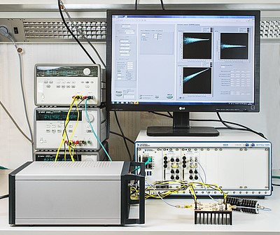
The used measurement setup is based on a National Instrument (NI) vector signal transceiver (VST) PXIe-5646R. For controlling the VST basic functions from NI are used. The models, which are used for linearization of the amplifier, as well as all required calculation for the models are realized in MATLAB. Fig. 1 shows a photo of the measurement setup based on the VST.
![]()
![]()
![]()
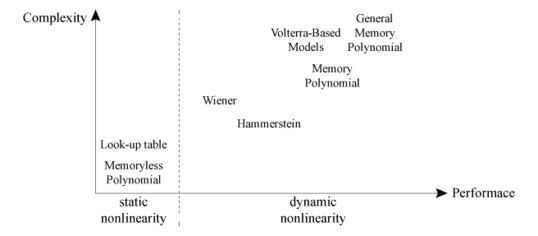
Fig. 1: Measurement setup for PA behavioral models and DPD An overview of the used structures of PA behavioral models is shown in Fig. 2.
![]()
![]()
![]()
Fig. 2: Structures for PA behavioral models and DPD The models are divided into memory and non-memory affiliated and can be differentiated in terms of their complexity and performance. Depending on the PA, the available hardware and the signal characteristics the behavioral model is chosen.
Waveform Engineering
Amplifier architectures are commonly complex circuits. Normally an amplifier is characterized by measuring input and output quantities and the direct current (DC) operation point. However, in some instances these quantities do not deliver enough knowledge to the developer about the grounds on which the performance of the power amplifier is based.
Furthermore, knowledge about the high frequency voltages and currents (waveforms) is important at all levels of the design process, e.g. for the verification of the circuit design and its compliance with the system requirements.
-
Concept of the In Situ measurement approach
Using the high frequency voltages \(V(t)\) and currents \(I(t)\) in time domain is a suitable approach for describing the behavior of non-linear radio frequency (RF) circuits. Fig. 17 shows the schematic of the measurement setup based on a sampling oscilloscope and a directional coupler. The measurement setup is realized as a microstrip technology circuit with a reference plane set to a position on a microstrip line with a characteristic impedance of \(Z_0\) = 50 Ω. The directional coupler separates the incident and scattered waves of the DUT. The coupled voltages \(V_{3}(t)\) and \(V_{4}(t)\) are measured in time domain with the sampling oscilloscope.
![]()
![]()
![]()
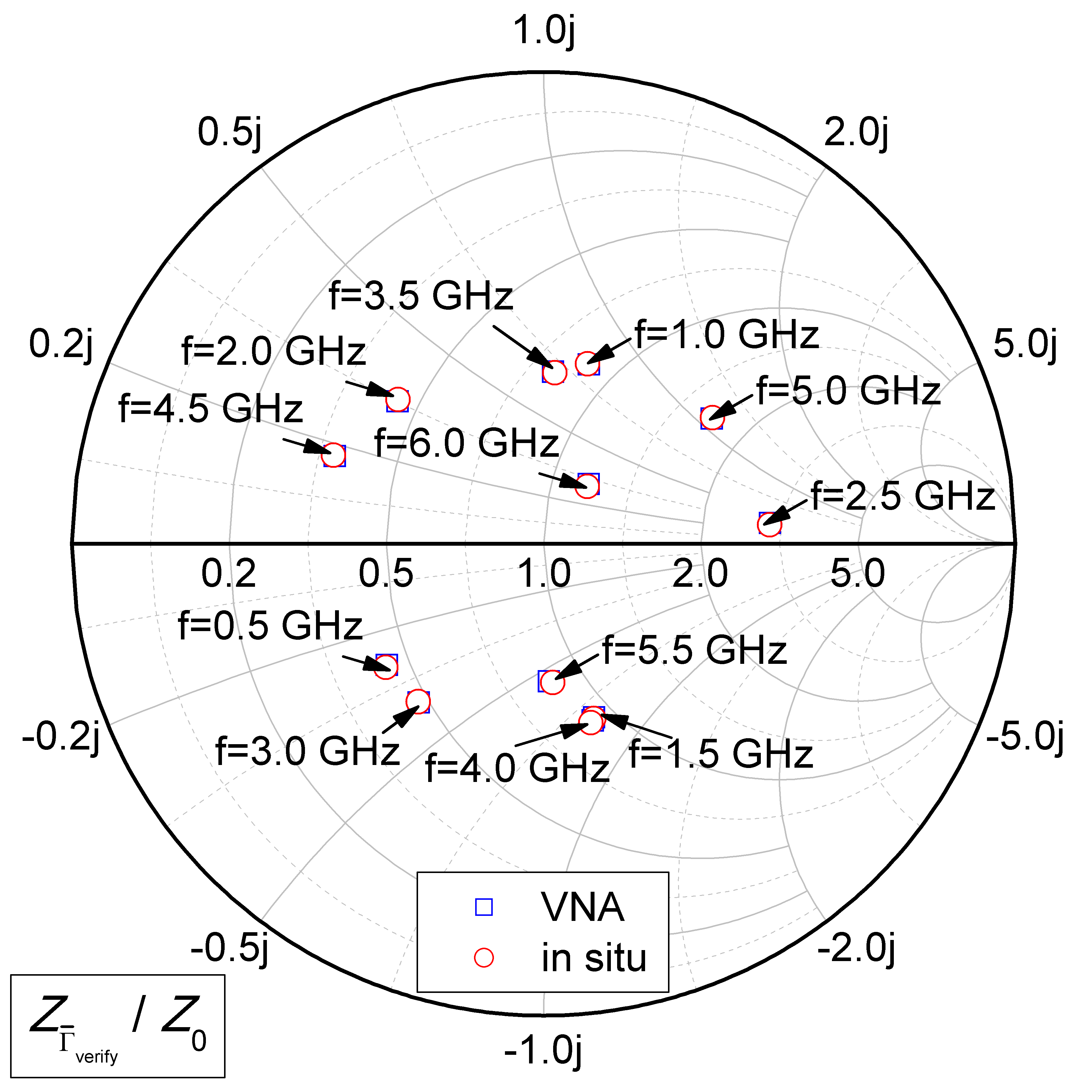
Fig. 17: Schematic of the in situ measurement setup To calculate \(V(t)\) and \(I(t)\) in the reference plane the measurement setup has to be calibrated taking into account the frequency response of the measurement setup (including the directional coupler and cables). In this context, a TOSM (Thru, Open, Short, Match) calibration procedure is enhanced by using calibration standards pre-characterized via the TRL (Thru, Reflect, Line) method. Therefore, the frequency of the RF source is swept to the distinct frequency points, i.e. to the fundamental frequency \(f_1\) and to the considered higher harmonics (up to 6\(f_1\)). The four-port coupler can be defined by means of the four-port / two-port reduction and thus can be described by a 2x2 error matrix E with coefficients \(e_{xy}\) for each frequency point, which are shown in Fig. 18.
![]()
![]()
![]()
Fig. 18: Signal flow graph of the error matrix E connected to the standards To determine the accuracy of the in situ measurement approach a comparison between a direct measurement and the in situ measurement with the coupler is conducted. For the measurements the sampling oscilloscope Agilent 86100B with module 86117B is used. As signal source the signal generator Agilent 4430C is utilized and synchronized to the oscilloscope. At first, the in situ determined impedance of a passive load in the reference plane is compared with a VNA (Rohde & Schwarz ZVA24) measurement. Furthermore, waveform is verified through direct measurements in comparison to the in situ measurement approach.
-
Verification of the In Situ measurement approach
1) Impedance
As a reference the impedance in the calibration plane is directly measured with a TRL calibrated VNA and obtained from the in situ measurement approach with the directional coupler. The test board is identical to the one of the calibration setup. Therefore, a verification reflection termination \({{\Gamma }_{\text{verify}}}\) is connected to the coupler, which translates to the measured \({{\tilde{\Gamma }}_{\text{verify}}}\) in the reference plane and its impedance \({{Z}_{{{{\tilde{\Gamma }}}_{\text{verify}}}}}\). The results for the normalized impedance \({{Z}_{{{{\tilde{\Gamma }}}_{\text{verify}}}}}/{{Z}_{0}}\) are presented in Fig. 19. The comparison between both methods in a frequency range of 0.5 GHz to 6 GHz shows a good agreement.
![]()
![]()
![]()
Fig. 19: Normalized measured impedance 2) Waveform
Furthermore, in order to exhibit the accuracy of the waveform measurement a test circuit is used, which consists of two diodes, one connected in series to a microstrip line and the other one connected to ground. At the left hand side of the circuit a directional coupler is embedded, which is an exact reproduction of the one on the calibration board. The RF source provides an available source power of \(P_{in}\) = 6 dBm with a frequency of \(f_1\) = 1 GHz. The resulting voltages \(V(t)\) in the reference plane are calculated in MATLAB for the in situ measurement approach as well as for a direct measurement with the sampling oscilloscope directly connected to the test circuit. A comparison of the results in Fig. 20 shows a good agreement of both measurements. The diodes clip and attenuate the input signal. As a result of the non-linear behavior of the diodes the signal contains higher harmonics. Thus, Fig. 20 indicates the functionality of the in situ waveform measurement system for the fundamental frequency and the higher harmonics.
![]()
![]()
![]()
Fig. 20: Voltage waveform for the test circuit at \(P_{in}\) = 6 dBm and \(f_1\) = 1 GHz
An application for the in situ measurement approach is the measurement of the interaction of the carrier and the peak amplifier in a Doherty amplifier, e.g., in the package plane of the transistor.
-
Application Doherty Amplifier
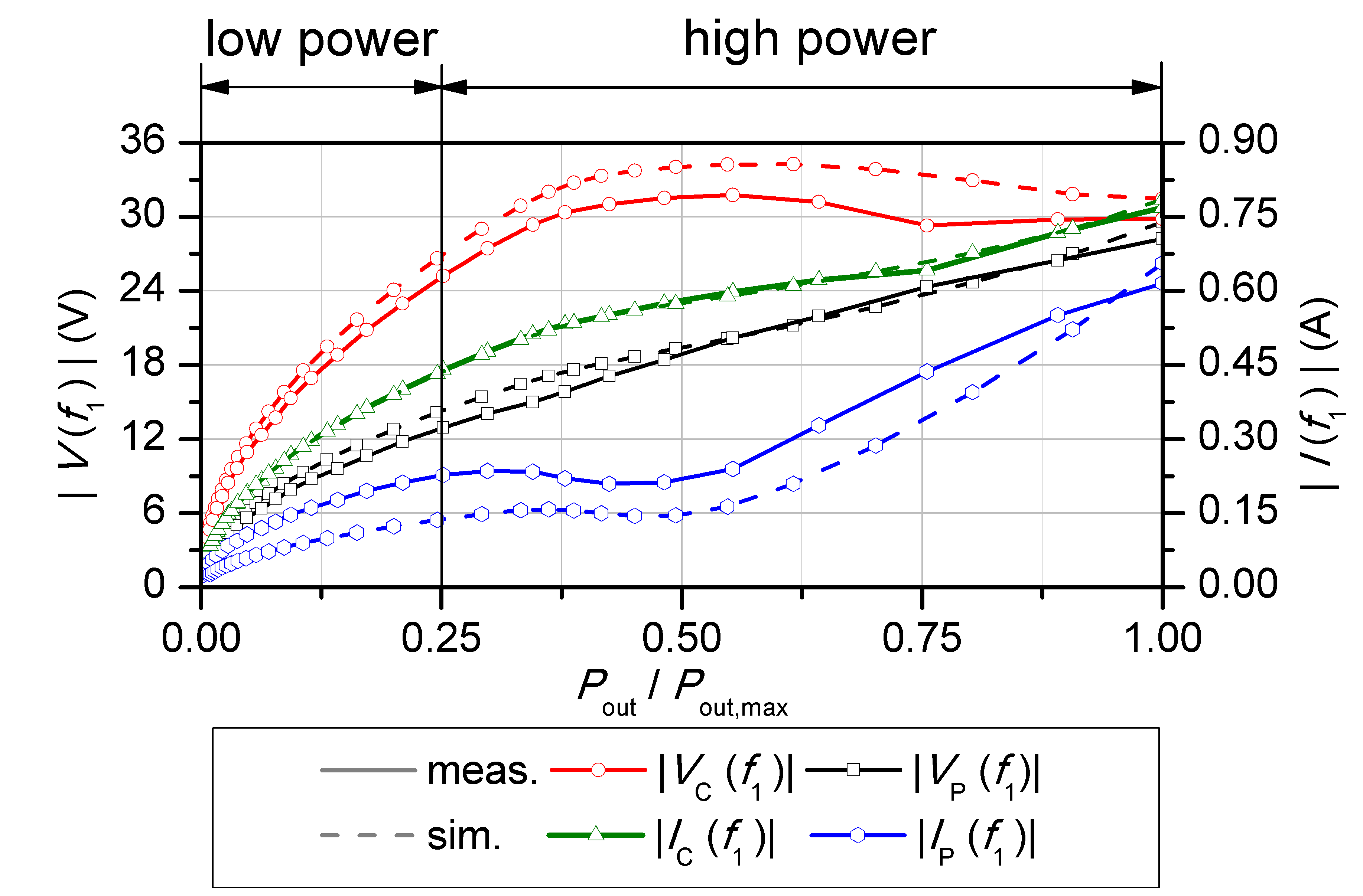
The interaction of the carrier and the peak amplifier can be described by the fundamental high frequency voltages and currents. Hence, Fig. 21 shows the relationship of the magnitude of the high frequency voltages (\(\left| {{V}_{C}}\left( {{f}_{1}} \right) \right|,\left| {{V}_{P}}\left( {{f}_{1}} \right) \right|)\) and currents \(\left| {{I}_{C}}\left( {{f}_{1}} \right) \right|,\left| {{I}_{P}}\left( {{f}_{1}} \right) \right|)\)) at \(f_1\) in the reference plane of the carrier and the peak amplifier over the normalized output power \(P_{out}=P_{out,max}\). In the high power range both amplifiers are active and the current of the carrier amplifier increases, while the voltage is approximately constant, which results in the high efficiency in this range. In general, a satisfying agreement between simulation and measurement exists. However, there is still some potential for improving the load modulation with help of the in situ measurements in a proceeding development process.
![]()
![]()
![]()
Fig. 21: Simulated and measured magnitudes of the voltages and currents at fundamental frequency for the carrier and the peak amplifier
Responsible Research Assistants


Prof. Dr.-Ing. Bernd Geck
Professorinnen und Professoren
Telefon
E-Mail
Adresse
Appelstraße 9a
30167 Hannover
30167 Hannover
Gebäude
Raum
Prof. Dr.-Ing. Bernd Geck
Professorinnen und Professoren
Telefon
E-Mail
References
[1] S. Probst, E. Denicke, B. Geck (2017): In Situ Waveform Measurements within a Doherty Power Amplifier under Operational Conditions, IEEE Transaction on Microwave Theory and Techniques, Vol. 65, No. 6, pp. 2192 - 2200, June 2017 DOI: 10.1109/TMTT.2017.2651809
[2] S. Probst, B. Geck (2015): In Situ Waveform Measurement Approach within an Inverse Class F GaN Power Amplifier, International Workshop on Integrated Nonlinear Microwave and Millimetre-wave Ciruits 2015 (INMMiC 2015), Taormina (Messina), Italy, October 1-2, 2015
DOI: 10.1109/INMMIC.2015.7330360


