In a load modulated amplifier the resistance \(R_{opt}\) which is seen by the transistors internal current source plane, is increased by \(1/x\) at low power levels, where \(0<x<1\) such that the voltage swing is maximized at all output power levels. Fig. 1 shows the operation principle of the load modulation amplifier assuming that the transistor is a perfect transconductor.

A possibility to change the \(R_{opt}\) is an adaptive output matching network. Fig. 2 shows an inverse L matching network with a tunable capacitance and inductance, which is used to vary the impedance \(Z_{opt,A}\) , respectively the \(R_{opt}\) at the internal current source plane.

In microstrip technology inductances are preferable realized as capacitances. Therefore, the series inductance is converted to a shunt capacitance with two \(λ/4\)-transformers (compare Fig. 3).


The tunable capacitance can be implemented as a parallel circuit of switched capacitors. The switches are realized using MEMS from RADANT of the type RMSW220HP. The RADANT MEMS has a long durability with >1 billion cycles at 40 dBm cold-switched. Furthermore, the MEMS offers the advantage of a good DC/RF isolation without additional components.
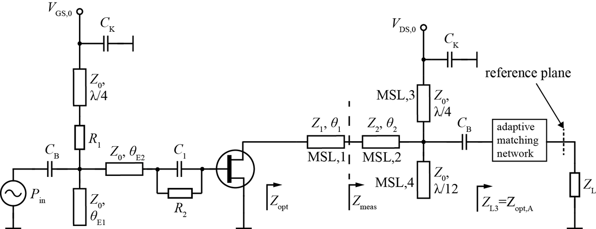
Before starting the design of the adaptive matching network, the MEMS are characterized with a vector network analyzer. With these measurements a S-Parameter model of the MEMS is generated to design the matching network. Fig. 4 shows the schematic of the developed adaptive matching network for the fundamental frequency \(f_0\) = 800 MHz. The matching network consists of eight MEMS, that provide 2^8=256 impedance states, but not all states are required and used for the load modulation.
For the state where all switches are turned off the impedance \(Z_{opt,A}\) is transformed with the offset capacitance \(C_{1offset}\) and \(C_{1offset}\). So that in this state (0-dB-back-off) \(Z_{opt,A}\) can correspond for example to an optimal impedance for the maximum output power of an amplifier.


With the objective of an application in a power amplifier for efficiency enhancement, the impedance range is chosen to be small for a refined resolution in the area of the optimal load impedance of the power amplifier. The simulation and measurement results for impedance \(Z_{meas}\) (compare Fig. 6) are shown in Fig. 5. Both, measurement and simulation results, cover the required impedance range that is needed for the load modulation.


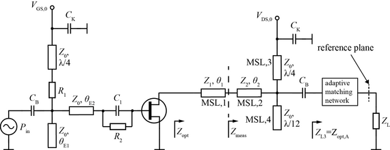
The schematic of the developed inverse class F power amplifier is shown in Fig. 6. The fundamental wave of an inverse class F power amplifier is terminated by \(Z_{opt}\) in the transistors package plane. Furthermore, the matching network provides high impedance at even harmonics and low impedance at odd harmonics. In this case, the second and third harmonic are terminated. The matching network is designed as an adaptive inverse L matching network based on MEMS switched capacitors for \(f_0\). By changing the capacity \(C_{1var}\) and \(C_{2var}\) of the matching network (shown in Fig. 4), the load impedance \(Z_L\) = 50 Ω is matched to the optimum impedance \(Z_{opt,A}\). The impedance \(Z_{opt,A}\) is tunable by the adaptive MEMS matching network and is transformed to \(Z_{opt}\) by the microstrip lines MSL,1 and MSL,2 with the electrical lengths \(θ_1\) and \(θ_2\). The termination of the second harmonic is realized with a \(λ_{f0}/4\) short-circuited stub at \(f_0\).The short is transformed by the microstrip lines MSL,1 and MSL,2 in an open at the drain of the transistor. The \(λ_{f0}/4\)-microstrip line serves as DC supply of the drain source voltage \(V_{DS,0}\). For the third harmonic a \(λ_{f0}/12\)-open-circuited stub is placed after the microstrip lines MSL,1 and MSL,2 to provide a short for the third harmonic at the drain of the transistor.

In Fig. 7 the PAE-envelop of an Class F power amplifier with the use of an adaptive matching network shows an efficiency enhancement compared to an Class F power amplifier without an adaptive matching. At 10-dB-back-off an efficiency enhancement of approximated 20 pp in comparison to the PAE of the fundamental state is achieved. In the fundamental state the power amplifier achieves the maximum output power of 40 dBm.


References
[1] S. Probst, B. Lüeers, B. Geck (2016): Load Modulation with an Adaptive matching Network Based on MEMS für Efficiency Enhancement of an Inverse Class-F power Amplifier, German Microwave Conference (GeMiC 2016), Bochum, Germany, March 14-16, 2016 DOI: 10.1109/GEMIC.2016.7461585


